


产品描述
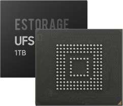
The QCN-4024-0-105DRQFN-MT-07-0 is an advanced RF (Radio Frequency) front-end integrated circuit (IC), likely designed for wireless communication systems that operate at high frequencies. It is used to manage signal amplification, filtering, and switching in various applications, such as mobile communications, Wi-Fi, and IoT devices. The IC is housed in a 105-pin DRQFN (Dual Row Quad Flat No-lead) package, which is compact and well-suited for high-density printed circuit board (PCB) layouts, making it ideal for space-constrained designs.
规格参数
Frequency Range:
Likely designed to operate in the GHz range, covering bands such as 2.4 GHz and 5 GHz for Wi-Fi, and potentially sub-6 GHz bands for 4G/5G mobile communications.
Supply Voltage (Vcc):
Operates on low voltages, typically in the range of 1.8V to 3.3V, depending on specific use case and configuration.
Amplification Gain:
LNA Gain: Generally between 10 dB and 30 dB, helping to improve reception of weak signals.
PA Gain: Typically around 15 dB to 30 dB, to ensure effective transmission of outgoing signals.
Noise Figure (NF):
Low noise figure (1.0 to 2.5 dB), ensuring minimal signal degradation and maintaining a high signal-to-noise ratio (SNR) for optimal communication performance.
Impedance:
Standard 50-ohm impedance, which is typical for RF systems, ensuring minimal signal loss and efficient signal matching with antennas and other components.
Switching Time:
Fast switching between different bands or modes (e.g., Tx/Rx), usually in the microsecond range, enabling rapid communication transitions in high-speed systems.
ESD Protection:
Equipped with Electrostatic Discharge (ESD) protection, likely in the range of 2 kV to 4 kV, safeguarding the IC from damage during handling and assembly.
Current Consumption:
Low power consumption, ranging between 10 mA to 100 mA depending on the active operation mode (amplifying, switching, etc.).